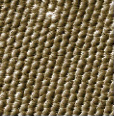
With the easyScan STM synthetic TiS2 single crystals have been investigated. On the 'as grown' material holes are observed on a large scan size.
Closer examination (cross section) reveals that the depth of the holes amounts to about 4 Angstroem which corresponds to a single atomic layer.
The STM experiments were performed under ambient conditions using mechanically prepared Pt-Ir tips. Typical tunneling parameters of 3.8 nA tunneling current and 180 mV GapVoltage were applied.

STM measurements on TiS2 single crystal (raw data)

