Electrostatic force microscopy (EFM) is an electrical mode in atomic force microscopy to map variations in the sample’s electric field and reveal information about the surface potential and charge distribution.
Electrostatic force microscopy or EFM is a common electrical AFM mode that provides useful, qualitative information on electric field gradients of a sample surface, thus providing a mechanism of contrast related to the sample electrical properties. EFM operates in amplitude modulation mode, a type of dynamic force mode where a cantilever with a thin electrically conductive coating is driven at its resonance frequency (this mode is also referred to as tapping mode). These cantilevers are inexpensive and commercially available.
Because the oscillating cantilever is sensitive to long-range electrostatic force gradients, EFM reveals qualitative information about the surface potential and charge distribution. The electrostatic interaction depends on the distance between the tip and sample, and the shift in resonance frequency of the cantilever monitors variations in the electrostatic field between tip and sample. As the potential difference between tip and sample increase, the resonance frequency drops resulting in a lower phase signal. Thus, a lower phase in the EFM channel indicates a larger potential difference between tip and sample.
EFM can operate in either a single-pass or a dual-pass method, similar to other electrical characterization methods such as Kelvin Probe Force Microscopy (KPFM). In the single pass method, the tip passes over the sample at a constant height while oscillating at resonance and with an application of a DC bias voltage between the tip and sample. The EFM phase and amplitude signal are thus collected together with topography. The single pass implementation of EFM can be useful for very flat samples. Single pass should be used with caution for rough samples or those with a significant amount of topography as the tip may crash into the surface. For these kinds of surfaces, a dual pass setup is a better choice:
In the more common dual pass setup for EFM, the cantilever passes twice over every line in the image. During the first pass, the tip is in contact with the sample as it maps out the topography in amplitude modulation mode. The tip is then lifted over the sample for the second pass by an amount prescribed by the user (this lift height parameter is optimized during every image and is typically only a few or tens of nanometers) and follows the contours of the topography but at a gap between tip and sample. During this second pass, the piezo continues to oscillate the cantilever at its resonance frequency. Additionally, a DC bias is applied between the tip and sample in this elevated pass so that the electrostatic forces shift the resonance frequency, amplitude, and phase. The resulting EFM amplitude and phase signal are mapped simultaneously with the topography, providing a useful correlation between the surface structure and its electrical properties. This implementation of EFM provides the best spatial resolution and thus superior correlation of the EFM image with surface topography. However, a slow scan rate coupled with the double pass measurements can lead to long acquisition times for a single image in dual pass mode.
Examples of EFM
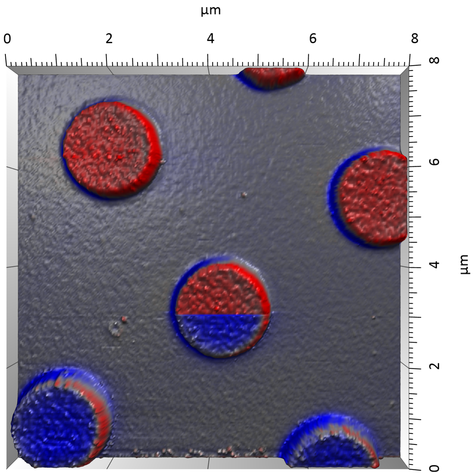
Aluminum dots were deposited on a gold substrate and imaged with EFM at different bias voltages between tip and sample to probe the different work functions of these two metals. The EFM image below shows the EFM phase contrast overlaid onto the 3D topography where the top half was collected with a +3V bias voltage and the bottom half of the image collected with a -3V bias voltage. The EFM phase difference between two metals with different work functions (like aluminium and gold in this sample) increases with increasing tip voltage. This is shown in the EFM phase image of this sample. At +3V, the phase on the aluminum is higher (red) as shown in the top half of the image. When the voltage is switched to -3V, the contrast inverts where now the phase on the aluminum pillars is low (blue) as shown in the bottom half of the image. This contrast inversion is due to the change in bias voltage which also indicates a change in potential difference between the two materials and the tip.


