Atomic force microscopy is one of the most popular techniques for metrology measurements such as surface roughness due to its ability to quantitatively measure the x, y, and z direction with nanoscale resolution.
AFM is one of the few tools that is able to quantitatively measure all 3 dimensions of a surface: lateral (x and y) and height (z). Unlike other high resolution microscopic characterization methods that rely on interactions of electrons with a material, in AFM there is a mechanical contact between a tip and sample enabling an accurate measurement of sample topography and surface texture. With a resolution of 5-10nm laterally and sub-nanometer vertically, AFM is a powerful measurement instrument for quantitative measurements of a surface. This powerful quantitative measurement is coupled with flexibility in sample surface: there are no requirements on a sample to be able to be measured by AFM except that it fits into the instrument. Quantitative measurements of sample topography enable important metrological measurements such as roughness profile, finding irregularities on the surface, as well as more advanced measurements such as skewness and kurtosis.
There are multiple mode available in atomic force microscopy to perform surface roughness measurements, which differ by contact type. The simplest mode is contact mode, where the tip is “dragged” across the surface at a constant cantilever deflection. The user defines the load at which the tip is “dragged” across the surface so that a heavier load can be selected for stiff, robust materials and a lighter load for softer materials. A feedback loop on the z piezo in the instrument then keeps the cantilever deflection constant throughout the image. The topography information is provided through the z piezo motion.
A gentler mode to measure surface topography (and thus surface roughness) is tapping mode. This is a dynamic mode where the tip is oscillated at a resonance frequency, and now the tip gently interacts with the surface at a constant amplitude of oscillation. The user defines the amplitude of oscillation at which the tip images the surface so that a larger amplitude can be selected for stiff, robust materials and a smaller amplitude for softer materials. A feedback loop on the z piezo in the instrument then keeps the cantilever amplitude of oscillation constant throughout the image. The topography information is provided through this z piezo motion. With these two modes, practically any surface topography can be imaged from soft biological cells, to polymers, to stiffer semiconductors and metals.
Various parameters exist to quantify the roughness of a surface. The roughness value can be calculated from either a cross-sectional profile (line) or a surface (area). The most common roughness parameters rely on calculation of the vertical deviation from a mean line or plane. For this reason, only instruments that provide a quantitative measure of z can provide data that be analyzed for roughness. Images that give an “impression” of three dimensions, but where the third dimension is not quantified in height (e.g. SEM images), cannot be analyzed for a quantitative roughness.
The two most common roughness parameters that are calculated are an arithmetical mean deviation from the mean and a root mean square mean deviation for the mean. For an image where the area is being analyzed, the arithmetical mean is called Sa and is defined as \[\frac{1}{n}\sum_{i=1}^{n}\left | y_{i} \right |\] Similarly, the RMS roughness is defined as Sq and is defined as \[\sqrt{\frac{1}{n}\sum_{i=1}^{n}y_{i}^{2}}\]
More sophisticated roughness measurements are also possible. For example, the skewness of a sample, which gives a measure of the asymmetry of the surface topography, can be measured and is defined as \[\frac{1}{nRq^3}\sum_{i=1}^{n}y_{i}^{3}\] Kurtosis gives information on the tails of the distribution of z values on the surface and is defined as \[\frac{1}{nRq^4}\sum_{i=1}^{n}y_{i}^{4}\] In all these definitions y is the height (z) at a given pixel (i) in the image.
Example of topography measurement with AFM
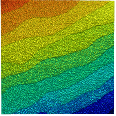
Part of the utility of atomic force microscopy as a metrological tool is its remarkable resolution in x, y, and z. Here is an AFM image collected of strontium titanate (SrTiO3), an oxide of titanium and strontium exhibiting a perovskite structure, which is used as a substrate for growth of oxide-based thin films and high temperature superconductors. This material forms a layered structure where the layers are only a few angstroms thick. AFM easily handles such a material and imaging these structures. In this 1.1µm x 1.1µm image, the strontium titanate layers are easy to observe. Each layer has an RMS roughness of approximately 0.125 nanometers caused by a non-ideal termination process during sample preparation. Below the image is shown a cross-sectional profile drawn across the image as well as a histogram binning the number of pixels at each sample height. In both the cross-sectional profile and histogram, layer thicknesses of approximately 4 angstroms are clearly observed revealing AFM’s remarkable resolution in z.

Example of surface roughness measurement
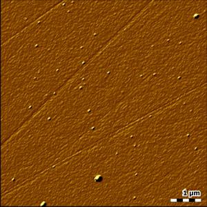
For some applications, sapphire or glass surfaces need to be polished down to sub-nanometer roughness. The image obtained here show polishing marks in and small contamination particles on the surface. The image was recorded in dynamic mode.
System: NaniteAFM with 10µm scan range connected to a C3000 controller
Cantilever: NCLAuD (Nanosensors)
Image processing: Nanosurf Report software
Sa = 0.12nm
The particles on the surface cause large values for the skewness and kurtosis of 49 and 2770, respectively.


