Nanosurf AFMs are used for applications ranging from material characterizations to biological samples like live cells. On this page you can browse the gallery of all our published atomic force microscopy images. All AFM images in this gallery were measured with a Nanosurf AFM. For in-depth articles of specific applications, visit the application notes page.
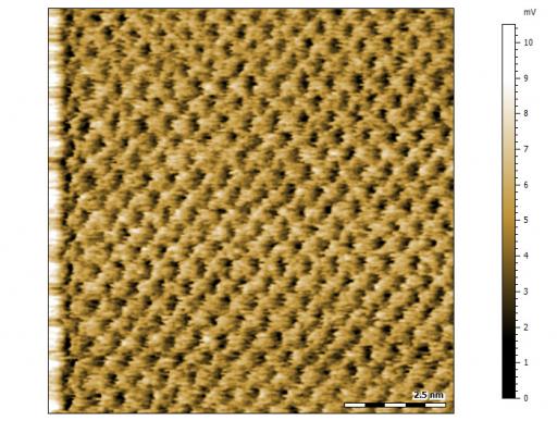
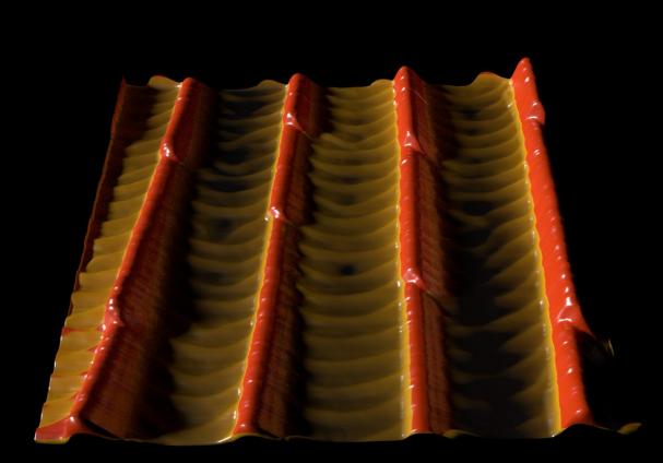
HOPG topography recorded in static mode on DriveAFM
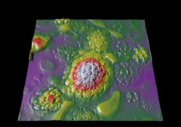
Mouse fibroblasts in cell culture medium
Performing Bio-AFM on live cells
Morphological characterization of various PDINO, TiOx, and PDINO:TiOx blend films
WaveMode image of mouse tail collagen
Thermal Lithography at PVAC thin film
Moiré super lattice of twisted graphene on hBN
Embryonic mouse fibroblasts
Trimeric arrangement of bacteriorhodopsin (BR) proteins and substructures
Cells imaged in medium with photothermal excitation and AC40 cantilever
HeLa cells in culture medium
PFM amplitude on 2D ferroelectric CuInP2S6 on Si
Force mapping on polymer blend (SBS-PS), Hertz model
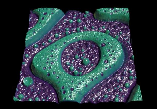
PS-Pb-PS triblock copolymer thin film on mica imaged at 20 Hz line rate
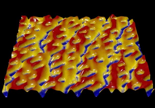
AFM topography of SiC showing 1.5 nm steps on its surface
TipCheck sample with CleanDrive excitation
Topography of an HOPG surface imaged in air
Atomic grid on mica measured with lateral force microscopy
MFM and topography on artificial spin ice
Quality control of CVD-grown graphene flakes on post-oxidized copper measured by fric...
3D topography of a grating structure with 390 nm deep trenches and an aspect ratio of...
Magnetic force microscopy of thin permalloy film with stripe domains
High-resolution topography image of double-stranded DNA (dsDNA) adsorbed to mica in b...
MFM images of a Shakti lattice
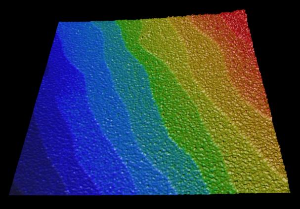
Topography of SrTiO3 in dynamic mode
Magnetic force microscopy of digital backup tape
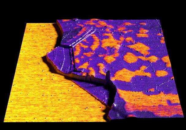
Topography on multilayer graphene
KPFM on multilayer graphene
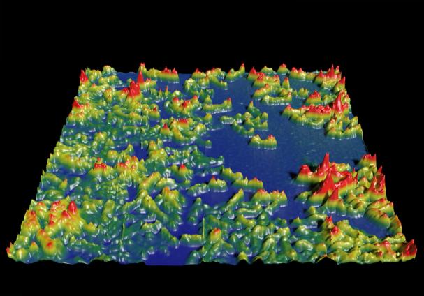
Topography of MoS2 monolayer
MoS2 monolayer: 3D topography overlaid with KPFM signal
Topography of locally deposited charges on an insulating oxide surface
KPFM of locally deposited charges on an insulating oxide surface
Topography of an integrated circuit structure with multiple transistor contacts
Conductive AFM of an integrated circuit structure with multiple transistor contacts
Out of plane PFM on Lithium Niobate
Electrostatic force (EFM) measurements on aluminum dots deposited on gold
Topography of polished stainless steel
Magnetic force microscopy on polished stainless steel
KPFM on polished stainless steel
Electrochemical AFM with rod-like samples: Cu deposition on a commercial Pt electrode
Force mapping of living cultured cells
AFM imaging of type I collagen fibrils
Dynamic mode AFM of pyrene nanosheets
Dynamic mode AFM of polished sapphire
AFM force spectroscopy on a polymer blend
AFM phase image of a polymer blend
AFM topography of a living HeLa cell
High resolution imaging of the cytoplasmic side of bacteriorhodopsin
Colloidal spectroscopy with FluidFM®
Single Cell Force Spectroscopy
Spotting and lithography with FluidFM
Topography analysis of ePTFE membrane using AFM
Magnesium fluoride coating
Photoresin Interference Grid
Topography of solar cell layers
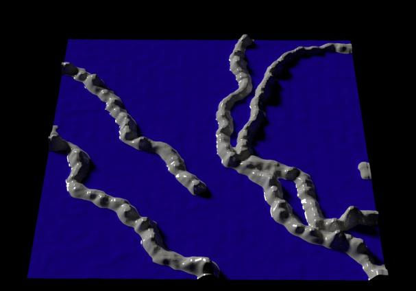
Screw dislocations in GaN
Dynamic mode AFM on pentacene film on TiO2
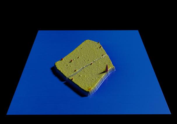
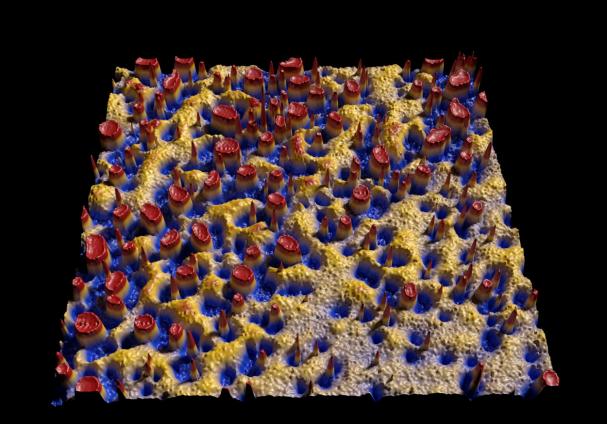
Morphology analysis of paper
Contact mode AFM of polished ceramic plate used in dentistry
Dynamic mode AFM of human hair
MFM of bits on a harddisk
AFM image of quantum dots
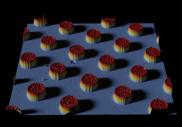
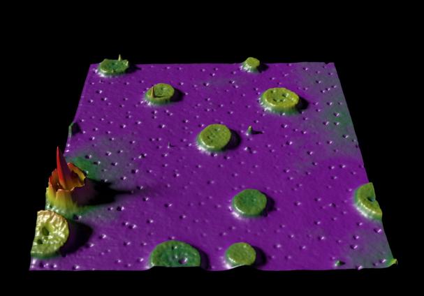
AFM images of gold film on ceramic grains
AFM image of butterfly wings
Static force AFM of stainless steel
Graphene imaged in Kelvin probe force microscopy (KPFM) mode
Geobacter bacterium on gold substrate imaged in dynamic force mode
SBS-PS polymer blend imaged in phase contrast mode
Quantum dots on potassium bromide (KBr) imaged in dynamic force mode
Magnetic tape imaged in magnetic force microscopy (MFM) mode
Gold (Au111) imaged in scanning tunneling microscopy (STM) mode
Graphene like C3N imaged in scanning thermal microscopy (sThM) mode
dsDNA imaged in dynamic force mode
Aluminum pillars on gold imaged in Kelvin force microscopy (KPFM) mode
SBRS-PMMA polymer blend imaged in force modulation mode
Mill moth wing imaged in static force mode
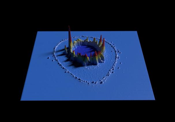
Laser ablation crater in TiO2 imaged in dynamic force mode
SBS-PMMA polyer blend imaged in lateral force microscopy (LFM) mode
SBR-PMMA polymer blend imaged in phase contrast mode
DVD imaged in dynamic force mode
SrTiO3 topography measured in dynamic force mode
Scanning tunneling microscopy makes it possible to see individual atoms. Since STM is based on quantum tunneling, where a voltage difference (bias) is applied between the tip and the sample surface, it only is applicable to metal surfaces or other conducting materials. View this gallery of STM images for examples of different surfaces at atomic resolution (single atoms are discernible).
Carbon nanotubes on graphene-silicon carbide
Electrode surface modified with multilayers of Polyoxometalate
STM image of TaS2 surface
Atomic structure of a TiS2 surface
STM study of high temperature superconducting thin films
STM on polished copper surface
STM Study of Evaporated Au (111) Thin Film
STM on HOPG shows atomic resolution
Defects study and atomic structure of MoS2 crystal with STM
Gold surface modification
STM imaging of 2D crystals
STM measurements on microfabricated grid

 of mouse fibroblasts in cell culture medium.")
. AFM recording (left) is shown as an overlay on the fluorescence image. For more information, see the full appnote at https://www.nanosurf.com/en/application/performing-bio-afm-on-live-cells")

. Measurement was performed with WaveMode in Studio. Scan size: 5um, scan speed 2.5 Hz line rate and 20 kHz WaveMode oscillation frequency.")

 phase image with scan size of: 190 x 190 nm²
Read more in the appplication note:
Evaluating AFM as an analysis tool for graphene")

 and phase (right) recorded in PFM imaging mode at the contact resonance frequency. Image size: 154 nm x 154 nm. Sample courtesy: Nanoelectronics group, TIFR, India.")
 proteins
and substructures within the BR molecules. Inset: correlation average of BR trimers. The red dashed lines
indicate a BR trimer.")


, Hertz model")
 and topography (bottom) of an unannealed PS-PB-PS triblock copolymer thin film on mica imaged at 20 Hz line rate using an USC-F1.2-k7.3 cantilever.")


.")

")


 on stainless steel (scan size: 80 µm, phase range: 10°)")

")

")
")
")

")

 for clarity.")


. The length of the fibers and the size-distribution of the knots can conveniently be analyzed using the measurement tools integrated in the Nanosurf control software.")
. The deflection image was recorded with a Nanosurf FlexAFM installed on a Zeiss Axiovert inverted microscope. Details of the cell's cytoskeleton are readily discernible through the cell membrane using AFM.")

adsorbed onto muscovite mica (scan size: 2 µm, height range: 1.4 nm).")

")
")
")
")
")
")
")
")
")
 has had a great impact on nanotechnology devlopment because of its demonstrated ability to fabricate nanostructures. Local oxidation of metallic surfaces by atomic force microscopy has shown to be a lithographic method for the fabrication of devices and patterning of structures at nanometer scale (scan size: 11 µm, height range: 10nm).")
.")
")
.")
.")
.")
.")
.")
 are particles whose size is limited to a few nanometers. More precisely, a Q-dot is a sphere with a radius of few nm that can confine an electron in zero-dimension; hence the name 'dot'. The AFM image shows quantum dots on monoatomic substrate terraces (scan size: 1 µm, height range: 3 nm).")
")
")
.")
")
")
")
")
 with a superimposed Charge Density Wave (CDW) lattice of about 3.5 × a0 (scan size: 11 nm, height range: 0.8 nm).
The CDW lattice is rotated 11° with respect to the atomic lattice.")
")
 thin films (scan size: 180 nm, height range: 12nm)")
")
")
")
.")
 oriented gold thin films it is possible to locally modify the surface by applying a voltage pulse to the STM tip (scan size: 127 nm, height range: 1 nm)")
")
")