The all-in-one STM microscope for an easy entry into the world of atoms
Overview
NaioSTM — The all-in-one STM microscope for easy entry into the world of atoms
Small mechanical loop provides excellent stability
Atomic resolution in 5 minutes
Tiny footprint, easy to store and transport
The first scanning tunneling microscope (STM) was developed in 1981 by Gerd Binnig and Heinrich Rohrer at the IBM Research Laboratory in Rüschlikon, Switzerland, for the first time making individual atoms directly visible to a small group of specialists. They were awarded the Nobel Prize in physics in 1986. In 1997, Nanosurf went one step further and brought single atoms to the classroom!
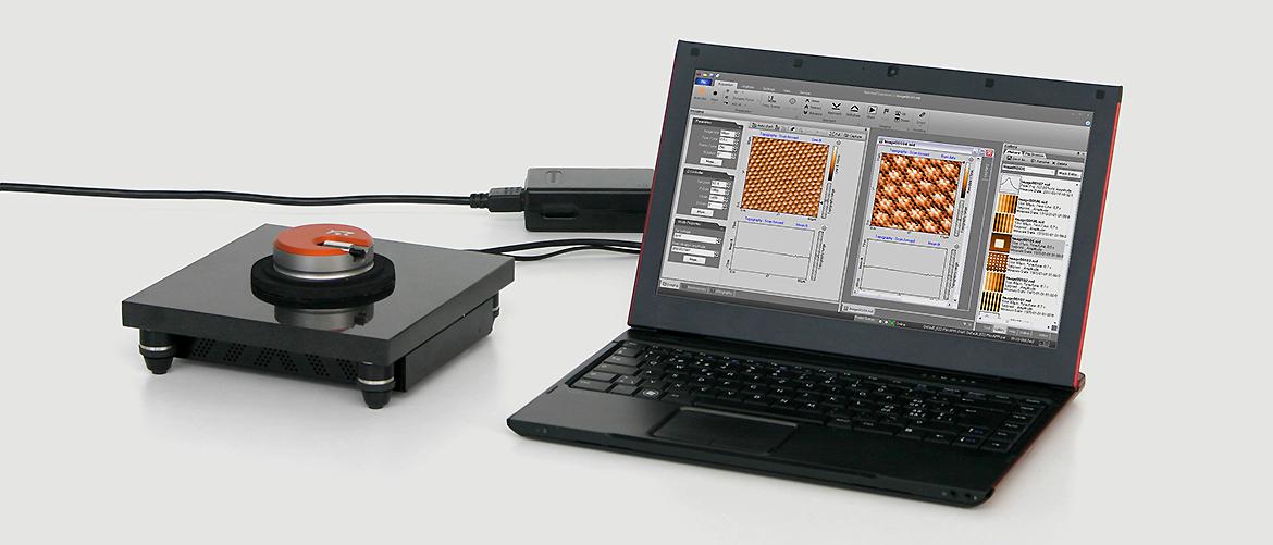
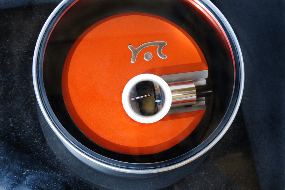
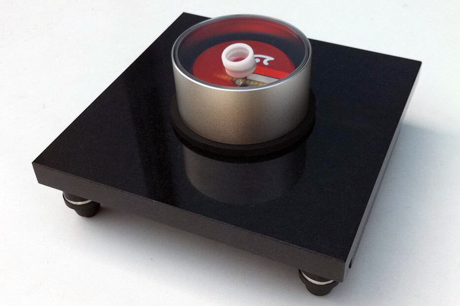
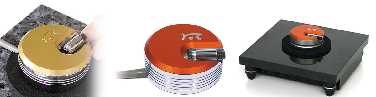
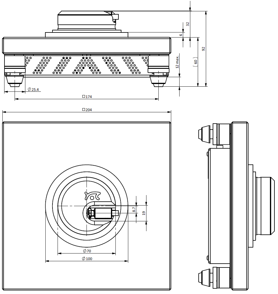
The NaioSTM is a scanning tunneling microscope that brings together scan head and controller in a single instrument for even simpler installation, maximized ease of use, and straightforward transportability. The setup is robust against vibrations and can be used to achieve atomic resolution on HOPG in standard classroom situations. With its 204 × 204 mm footprint it hardly takes up any workbench space.
Download the NaioSTM brochure
Smart design
The smart and purposeful design is perfectly suited to the needs of educational institutions: the system integrates scan head, controller, air-flow shielding with a magnifying glass to aid the initial approach, and vibration isolation on a heavy stone table. The very small mechanical loop of < 10 mm provides the stability to achieve atomic resolution on a coffee table or in a class room. The additional passive vibration isolation feet further protect measurements against disturbances, making the system very robust during operation. The system functions without high voltage, making it safe in unexperienced hands.
Ease of use
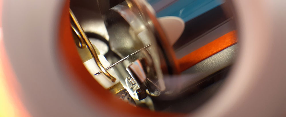
The smart design does not only provide good performance, but also makes the NaioSTM very easy to use. All that is required in terms of setup is to connect 2 cables: power and USB. It is safe to be handled by students or other users with no prior training, thanks to the lack of high voltage and its general robust design. Scanning tips are simply cut from Pt/lr wire, no hazardous substances are required to etch the tips. The process from setup up to seeing the first successful images can be achieved within a few minutes. The intuitive software is equipped with helpful wizards to guide you through the measurement process.

Dr. Koen Schouteden
Department of Physics and Astronomy
KU Leuven
Belgium
"While I used an identical system frequently in the past and hence know how well it works, it remains very nice to see the new system achieving atomic resolution in only few minutes upon first installation, with the pre-installed STM tip. And this time in a non-optimal environment: my office on the 5th floor! Also nice that the software and communication is working also on a MacBook (using Windows 10 in Parallels)." - Dr. Koen Schouteden
The number one STM solution in the field
Over more than 20 years and three development generations, Nanosurf's scanning tunneling microscope has become the number one STM solution in the field. Because of its clever composition, it is widely regarded as the logical choice for performing scanning tunneling microscopy in all kinds of educational settings and basic research, with almost 1500 instruments in operation around the world.
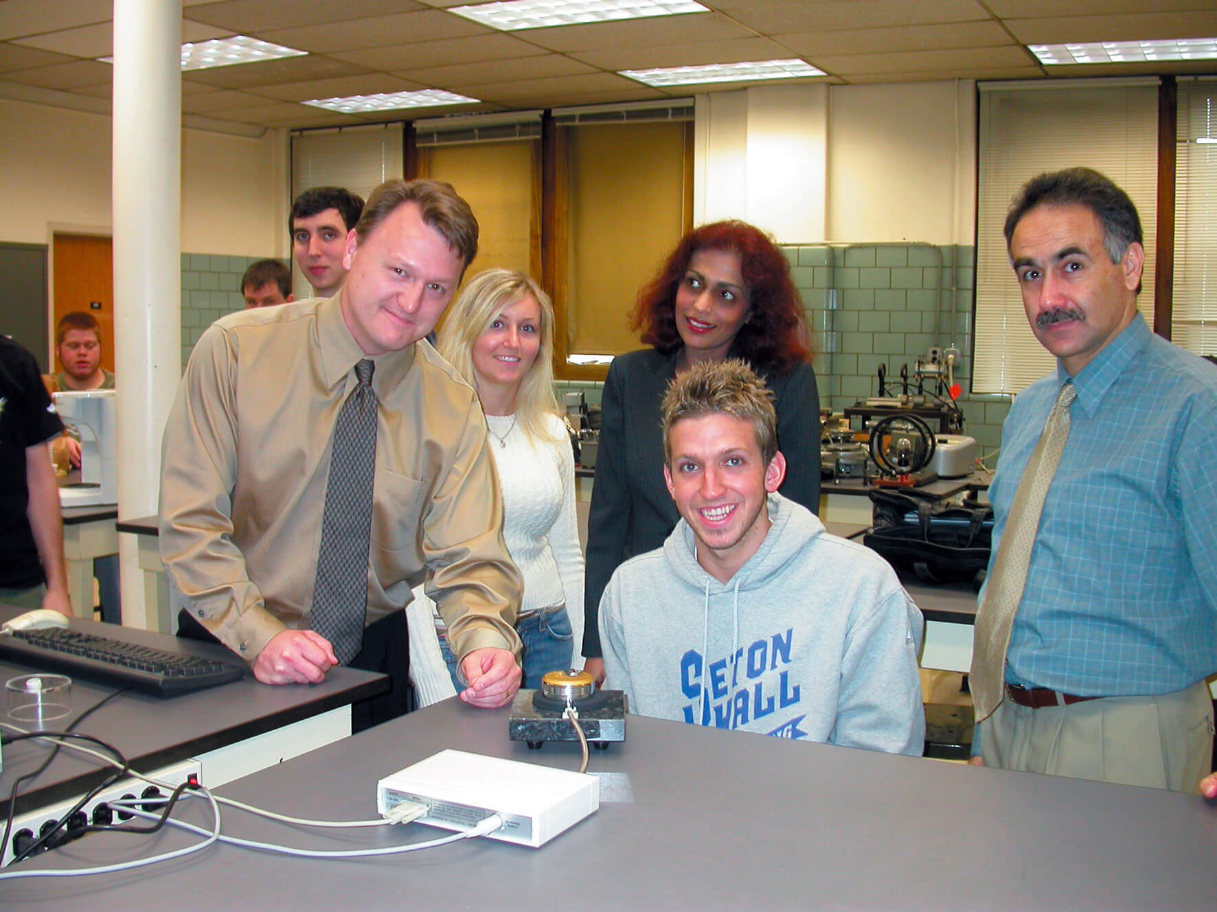
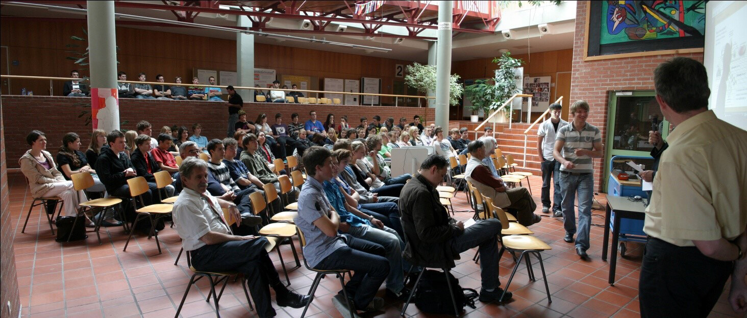
It is so easy to use, professors and teachers love to carry out practical demonstrations on the NaioSTM, and students find it highly motivating to be able to successfully perform hands-on experiments themselves, without long preparation.
Scanning tunneling microscopy is considered as one of the cornerstones of nanotechnology. Paired with the NaioAFM, Nanosurf brings nanotechnology on the atomic scale to the classroom, providing insights in the fields of physics, biology and chemistry.
Why is this STM so popular in the classroom?
- Teachers appreciate the ease of use of Nanosurf STMs, allowing them to offer quick and hassle-free classroom demonstrations to their students.
- Students are motivated by the rapid successes achieved when using the STMs themselves during hands-on training.
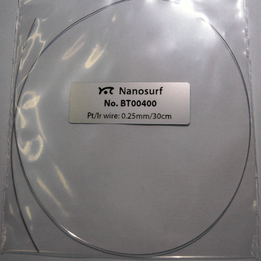
- Anyone can safely handle a Nanosurf STM, since the conducting tips are simply cut from Pt/Ir wire without requiring etching in hazardous substances.
NaioSTM imaging modes
This overview shows which modes the instrument is capable of. Some modes may require additional components or software options. For details, please view the brochure or contact us directly.
Imaging modes
Constant current (topography)
Constant height (current)
Spectroscopy modes
Current-voltage
Current-distance
Lithography modes
Patterning
Modification
System dimensions
")
")
")
")
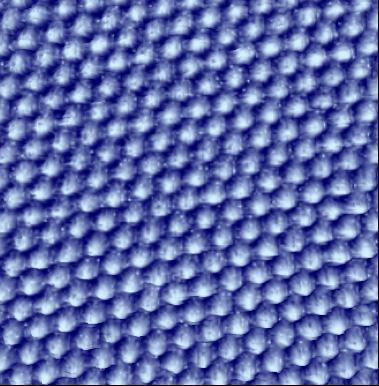
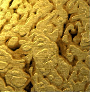
 thin films (scan size: 180 nm, height range: 12nm)")
")
.")
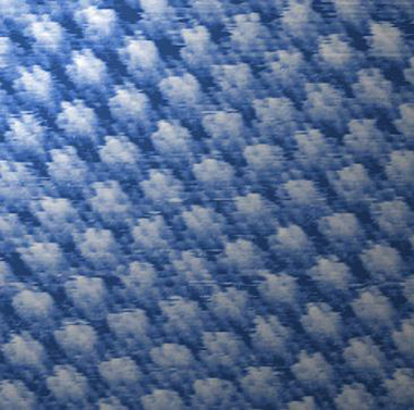
 oriented gold thin films it is possible to locally modify the surface by applying a voltage pulse to the STM tip (scan size: 127 nm, height range: 1 nm)")
")
")