Kelvin probe microscopy or KPFM is one member of a suite of electrical characterization methods available in scanning probe microscopy to map the surface potential or work function of samples.
KPFM provides information on the contact potential or work function of a sample surface, thus providing a mechanism of contrast related to the sample electrical properties. Work-function is defined in solid states physics as the energy needed to remove an electron from the Fermi level in a solid to vacuum; work function is thus a property of the surface, not the bulk. Therefore KPFM is a surface-sensitive method that probes the surface and near-surface only.
Kelvin probe force microscopy operates in amplitude modulation mode, a type of dynamic force mode where a cantilever with a thin electrically conductive coating is driven at its resonance frequency (this mode is also referred to as tapping mode). These cantilevers are inexpensive and commercially available.
KPFM can operate in either a single or dual pass setup. In the single-pass setup, the tip passes over the sample at a constant height. An AC voltage is applied to the cantilever during this pass, creating an oscillating electrostatic force between tip and sample, which is measured by a lock-in amplifier. A DC voltage is then applied to null the potential and thus prevent cantilever oscillation. This applied DC voltage is then mapped as a measure of the contact potential difference between tip and sample. This potential difference can also arise from a difference in work function between tip and sample. An advantage of the single pass mode is that the tip is closer to the sample so there is higher sensitivity and resolution in the Kelvin force measurement, but the spatial resolution may suffer. This implementation of KPFM is also the fastest (there is no feedback on the z signal) and also minimizes tip wear.
In the dual pass setup, the cantilever passes twice over every line in the image. During the first pass, the tip is in contact with the sample as it maps out the topography in amplitude modulation mode. The tip is then lifted over the sample for the second pass by an amount prescribed by the user (this lift height parameter is optimized during every image and is typically a few or tens of nanometers. Optimization entails a trade-off between having the tip as close to the sample as possible to avoid stray capacitance from the lever but not being too close as to crash into the sample). This second pass is similar to the single pass setup described above: the AC voltage is applied to the probe at its resonance frequency in order to drive it. This electrical actuation is in contrast to piezo actuation that is used to drive the cantilever for topography imaging in the first pass. When the sample surface potential is different than the potential of the probe, the resulting electrostatic forces causes mechanical oscillation of the cantilever. A DC voltage chosen through potential feedback loop is then applied to zero the difference in potential between tip and sample, which is recorded as the surface potential. A slow scan rate coupled with the double pass measurements can lead to long acquisition times for a single image in the dual-pass mode. However, this implementation of KPFM does provide the best spatial resolution and thus superior correlation of the KPFM image with surface topography. Quantitative KPFM measurements of the local sample work function is possible. However, this requires a model to describe the electrostatic interactions between tip and sample as well as knowing the work function of the tip.
Applications of KPFM
An example of a single pass KPFM measurement is shown below on a multi-layer graphene flake. These flakes were synthesized by mechanical exfoliation of graphite and subsequent transfer to a silicon-silicon dioxide substrate. A 3-dimensional 8mm x 8mm topographic map of the graphene flake surface is shown below. The coloring of this topographic map represents the KPFM signal, or an image of the contact potential during the image. Contrast that is purple or pink is high contact potential while contrast that is green is low contact potential. Through this contact potential map, the different electrical properties of the different thickness flakes is clearly evident as the thin flakes on top have high contact potential (blue coloring) while the other layer has a lower contact potential (green coloring). This data was collected by a CoreAFM.

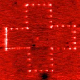
Another example of a dual pass KPFM measurement is shown below on an insulating oxide. In this sample, local charges were placed on the insulating oxide surface layer in a Swiss cross pattern. The topography image is shown on the left where there is no indication of any Swiss cross pattern. The KPFM image is shown on the right where the surface potential image provided by KPFM clearly reveals the pattern of charges.
The combination of electrical modes and magnetic force microscopy is also powerful, as illustrated for stainless steel that was imaged by KPFM and MFM. Kelvin probe force microscopy is available for the CoreAFM and FlexAFM product lines.