The method of piezoelectric force microscopy or piezoresponse force microscopy (PFM) described here is an electrical mode in the scanning probe microscopy family used to study the piezoelectric phenomenon of materials on the nanoscale. PFM measures nanoscale topography simultaneously with a material’s mechanical response in response to application of electrical voltage.
Piezolectricity is simply the electric charge that accumulates in certain solid materials and responds to mechanical stress. Many materials are piezoelectric. Certain crystals, ceramics, and biological materials such as teeth, bone, DNA, and various proteins. For biological samples, their innate piezoelectricity may be relevant for their mechanobiology. The piezoelectric effect results from the internal generation of electrical charge resulting from an applied mechanical force. The converse piezoelectric effect results from the internal generation of a mechanical strain resulting from an applied electrical field. Because atomic force microscopy is fundamentally based on an actual mechanical contact between tip and sample, it is uniquely suited to study this phenomenon in materials on the nanoscale.
Ferroelectrics are a subset of piezoelectrics and are also commonly studied with PFM. Ferroelectrics exhibit spontaneous electric polarization that can be reversed in direction by applying an electric field. In a material with ferroelectric domains, reversing the external field reverses the predominant orientation of the ferroelectric domains. Switching to a new direction lags behind the change in field. This effect is known as hysteresis. Ferroelectric properties are harnessed in many important applications for electronic devices such as sensors, actuators, detectors, and memory devices. PFM is a unique tool that enables the visualization of ferroelectric domains at micro and nano lengthscales.
PFM is based on the converse piezoelectric effect where a voltage is applied to the sample resulting in a sample extension. This mechanical extension of the sample is then measured in PFM. The sample extension or displacement measured in PFM is very small and measures only a few nanometers.
PFM is also used frequently to study ferroelectric domains. The applied bias voltage can switch regions of ferroelectric domains so that ferroelectric domain structure and formation can be explored with nanoscale resolution. In this way, topography and corresponding ferroelectric domains be imaged with nano or micro resolution.
PFM operates in static mode, where a conducting AFM probe scanned at constant force over the sample. A conducting probe is needed as a way of applying the bias voltage over the sample while scanning. Common electrically conducting coatings are platinum, gold, tungsten, and conductive diamond. These cantilevers are inexpensive and commercially available.
An AC voltage is applied between the AFM tip and sample surface to generate the converse piezoelectric field in the sample. The sample will either contract or expand due to this applied voltage resulting in a deflection of the PFM cantilever. This cantilever deflection is monitored with a standard photodiode detector and demodulated with a lock-in amplifier. Both the PFM amplitude and phase of the oscillating cantilever are monitored. The PFM amplitude signal provides information on the strength of the signal and thus the material’s piezoelectric tensor. The PFM phase signal provides information on the direction of polarization.
PFM is a non-destructive AFM method. It provides a high resolution measurement of a material’s piezoresponse with minimal sample preparation. However, image acquisition is often very slow in the tens of minutes. Also, tip wear can change the tip-sample interaction significantly thus affecting the PFM contrast. Unfortunately it is difficult to monitor tip wear directly so this can induce artifacts into the image.
Examples of Piezoelectric force microscopy
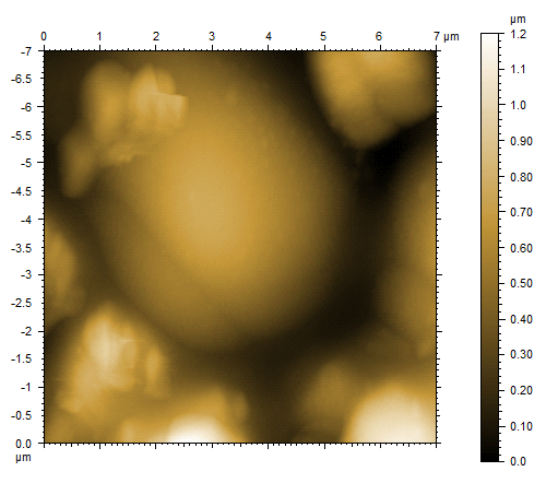
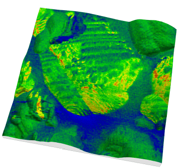
Piezoelectric materials are commonly used in transducer discs for loudspeakers, pressure transducers and contact microphones. The piezo layer on such discs is produced by a thick-film coating process and has a polycrystalline structure. Below is a 7µm x 7µm PFM image of a 100µm thick layer of a common piezo material, lead zirconate titanate (PZT). The topography image on the left shows the morphology of the polycrystalline material. The PFM phase signal is shown on the right revealing the ferroelectric domains in this sample.


Another example of piezoelectric force microscopy is shown below. Piezo sensors and mobile phones use a common optically transparent material called lithium niobite (LiNbO3). In this 10µm x 10µm image, the PFM phase signal is overlaid onto the topography where the coloring is now due to the PFM phase signal. In this image, a 7.5V AC voltage was applied to the cantilever-sample contact while imaging. In response, the sample periodically expands or shrinks either in phase or counter-phase to the excitation frequency. These piezoelectric domains are easily observed with the contrast from the PFM image.


