Molybdenum disulfide (MoS2) is one of the most commonly studied graphene-like 2D materials.[1] Atomically thin MoS2 is a semiconductor with unique electrical[2], optical[3], and mechanical[4] properties, which make it a useful material for piezoelectric[5], photovoltaic[6,7], and other optoelectronic applications[8].
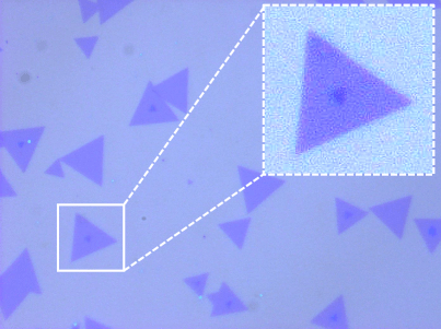
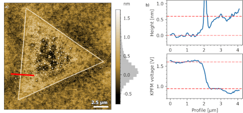
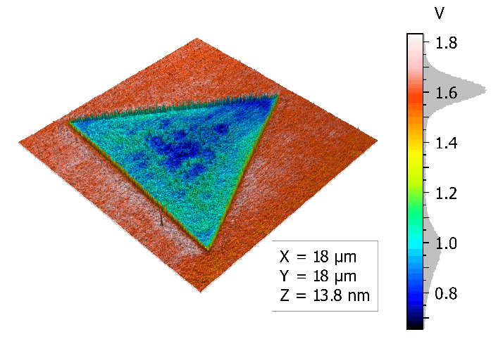
In this application note, monolayer MoS2 grown by chemical vapor deposition (CVD) was imaged with Kelvin probe force microscopy (KPFM) using a Flex-Axiom to study the contact potential difference variation on a single crystal.

Monolayers of MoS2 were grown on a silicon substrate by chemical vapor deposition.
Sample courtesy: University of Illinois – Urbana-Champlain

Measurements using the Flex-Axiom show a step height of 0.6 nm for the MoS2 monolayer. Concurrent KPFM measurements show a 650 mV contact potential difference between the monolayer and the SiO2 substrate.
Non-uniformity of the contact potential signal across the monolayer can inform about doping profiles and other surface defects.

All measurements were performed using a Flex-Axiom system equipped with a ANSCM-PA cantilever from AppNano. Images were processed using MountainsMap SPM.
For more information contact our application scientists
[1] Subbaiah, Y.P.V., et al., Advanced Functional Materials 26 (2016) 2046
[2] Mak, K.F., et al., Physical Review Letters 105 (2010) 136805
[3] Splendiani, A., et al., Nano Letters 10 (2010) 1271
[4] Akinwande, D., Nature Communications 5 (2014) 56787
[5] Wu, W., et al., Nature 514 (2014) 470
[6] Tsai, M.-L., et al., ACSNano 8 (2014) 8317
[7] Wi, S., et al., ACS Nano 8 (2014) 5270
[8] Sanne, A., et al., Nano Letters 15 (2015) 5039
Nanosurf application note AN01154

