Gallium nitride features some unique properties such as large band gap, strong interatomic bonds, and high thermal conductivity. Along the last decade, GaN has attracted great interests owing to its potential applications in high power and high frequency electronic devices as well as in blue LED devices.
GaN layers are usually grown by Metal Organic Chemical Vapor Deposition and the Molecular Beam Epitaxy methods.
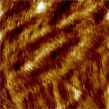
Sapphire is now the most commonly used substrate despite of its highly mismatched lattice and thermal expansion coefficients. As a consequence, the obtained GaN layers often contain an large number defects [4], mainly dislocations. The image shows a piece of GaN with steps and screw dislocations (holes). The goal is to count number of dislocations and step distribution.


