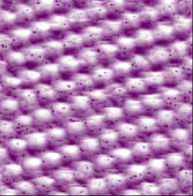
Natural MoS2 crystals were cleaved prior to the STM experiment. The measurements have been carried out under ambient conditions. Typical tunneling parameters were 1.6nA tunneling current and 0.35V gap voltage.

Some nanometre sized inclusions were found within the atomically resolved crystal lattice.

