Studies of MC2 capacitance by scanning microwave microscopy
Nanosurf's team of application scientists is always working on creating new interesting measurements for the benefit of the users of Nanosurf atomic force microscopes. The application notes we publish are written and edited by our global team of AFM Experts to provide you with example results in an easy to ready format and enough theoretical context to help novice users understand more complex measurement methods.
This application note examines the use of Scanning Microwave Microscopy (SMM) for studying the MC2 capacitance standard sample, highlighting its significance in nano-electrical characterization, particularly for the semiconductor and microelectronics industries.
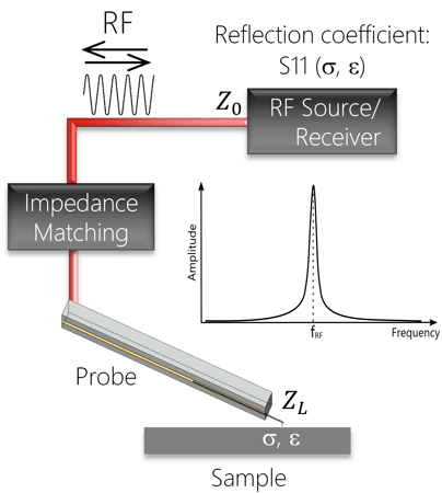
SMM, a technique that combines Atomic Force Microscopy (AFM) with microwave impedance measurements, is instrumental in assessing local electrical properties like conductance, dielectric constant, and dopant density.
Key learnings:
- SMM's Role in Nano-Electrical Characterization: Understand the importance of SMM in measuring local electrical properties, crucial for semiconductor research and development.
- Microwave Impedance Measurement with SMM: Learn about the measurement of local tip-sample microwave impedance using the S11 parameter, and its application in determining local capacitance and resistance.
- Capabilities of SMM in Material Analysis: Explore SMM's ability to measure a wide range of materials, including semiconductors, dielectrics, and metals, and its advantage over techniques like scanning capacitance microscopy (SCM).
- SMM Setup and Practical Applications: Gain insights into the typical SMM setup, involving a radio frequency wave source and receiver, and its practical applications in the semiconductor industry.
- Calibration and Quantitative Analysis in SMM: Understand the calibration procedures necessary for SMM to extract quantitative values for capacitance, resistance, and material parameters.
