In a good scanning tunneling microscopy image of highly oriented pyrolytic graphite (HOPG) you will see a pattern consisting of white, grey and black spots. To interpret the graphite STM image correctly: the bright spots mean higher tunneling current and dark spots mean lower tunneling current.

Out of the lattice model of graphite one can see that there are two different positions of the carbon atoms in the graphite crystal lattice (see e.g. R.C. Tatar et al. Phys Rev B 25 (1982) 4126).
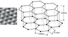
One with a neighbouring atom in the plane below (grey) and one without a neighbour in the lattice below (white). Consequently the electrical conductivity of the graphite surface varies locally slightly (different electronic density of states) so that the atoms without neighbours appear "higher" than the others (see e.g. I.P. Batra et al. Surf Sci 181 (1987) 126). This also causes the HOPG lattice constant between the bright 'hills' to have the higher value of 0.25nm than the nearest neighbour distance in the graphite lattice of 0.14nm.
For reference see e.g R.C. Tatar et al. Phys Rev B 25 (1982) 4126
View application note (PDF)