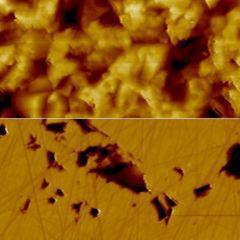
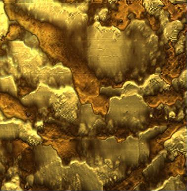
Atomic Force Microscope Images
Nanosurf AFMs are used for applications ranging from material characterizations to biological samples like live cells. On this page you can browse the gallery of all our published atomic force microscopy images. All AFM images in this gallery were measured with a Nanosurf AFM. For in-depth articles of specific applications, visit the application notes page.
[ Jump to STM image gallery ]

 of mouse fibroblasts in cell culture medium.")
. AFM recording (left) is shown as an overlay on the fluorescence image. For more information, see the full appnote at https://www.nanosurf.com/en/application/performing-bio-afm-on-live-cells")

. Measurement was performed with WaveMode in Studio. Scan size: 5um, scan speed 2.5 Hz line rate and 20 kHz WaveMode oscillation frequency.")

 phase image with scan size of: 190 x 190 nm²
Read more in the appplication note:
Evaluating AFM as an analysis tool for graphene")

 and phase (right) recorded in PFM imaging mode at the contact resonance frequency. Image size: 154 nm x 154 nm. Sample courtesy: Nanoelectronics group, TIFR, India.")
 proteins
and substructures within the BR molecules. Inset: correlation average of BR trimers. The red dashed lines
indicate a BR trimer.")


 are particles whose size is limited to a few nanometers. More precisely, a Q-dot is a sphere with a radius of few nm that can confine an electron in zero-dimension; hence the name")


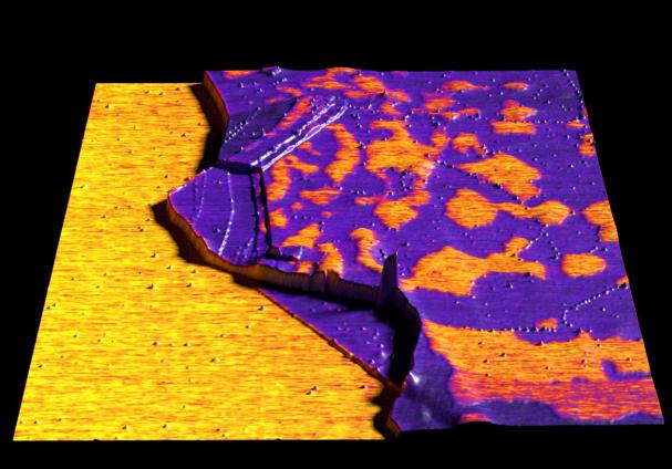
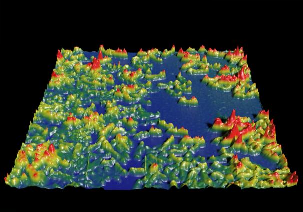
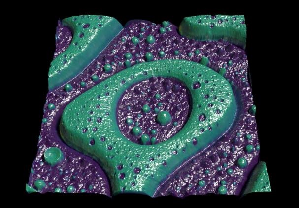
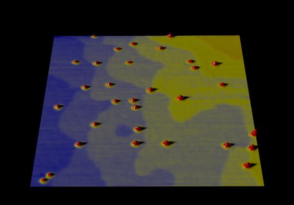
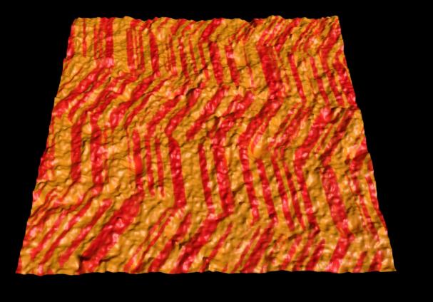
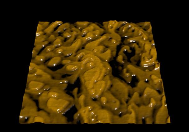
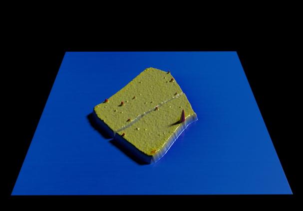
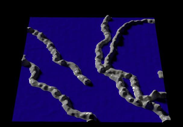
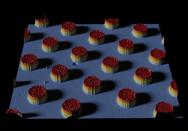
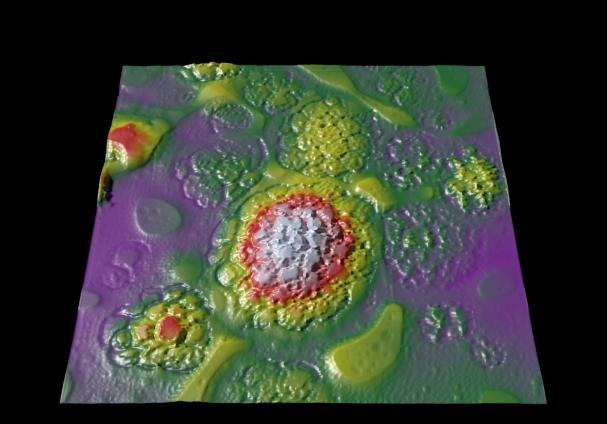
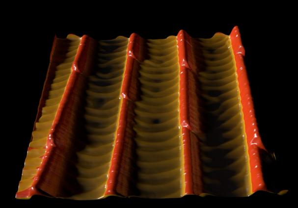
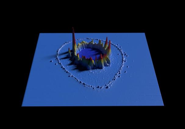
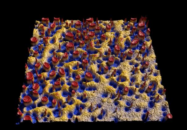
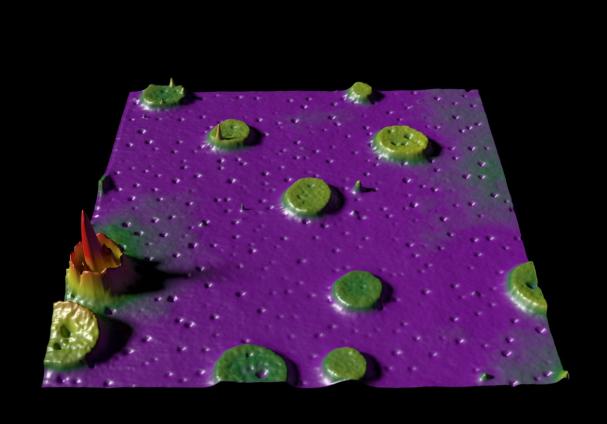
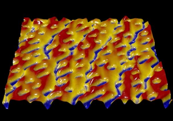
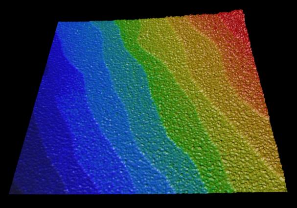
3D Renderings of Atomic Force Microscope Images
Scanning Tunneling Microscope Images
Scanning tunneling microscopy makes it possible to see individual atoms. Since STM is based on quantum tunneling, where a voltage difference (bias) is applied between the tip and the sample surface, it only is applicable to metal surfaces or other conducting materials. View this gallery of STM images for examples of different surfaces at atomic resolution (single atoms are discernible).
[ Jump to AFM image gallery ]


